In the past, I have designed several PCBs using RP2040 and RP2350. For those designs, I’ve used the “A”-suffix version, which were in QFN-60 package. Hence, it was having the same number of IO pins as the official Raspberry Pi Pico or Pico 2.
In last month (Sep 2025), I got a new project request and it was having too many IO peripherals connected. In the initial breadboard PoC, my client used MCP23017 to expand IO ports. We discussed and decided to try RP2350B, which is in QFN-80 package. It had 18 more GPIO pins than RP2350A, hence, we could eliminate the need of MCP23017 IO expander.
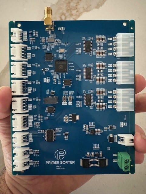
Key Features
- RP2350B Microcontroller from Raspberry Pi
- Dual Cortex-M33 or Hazard3 processors at 150 MHz
- 520 kB on-chip SRAM
- 48 GPIO pins in QFN-80 package
- 16MB (128Mbit) external SPI Flash, W25Q128J from Winbond
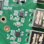
- Wi-Fi and Bluetooth 5.2, CYW43439 from Infineon (formerly Cypress)
- 3 x Stepper motor drivers, DRV8825 from Texas Instruments
- Several I2C, UART, and GPIO ports with using proper level shifters
- Power supply
- LM74502 from Texas Instruments for ON/OFF switching, overvoltage, and reverse-polarity protection
- TPSM863252 from Texas Instruments for 5V, 2A step-down converter
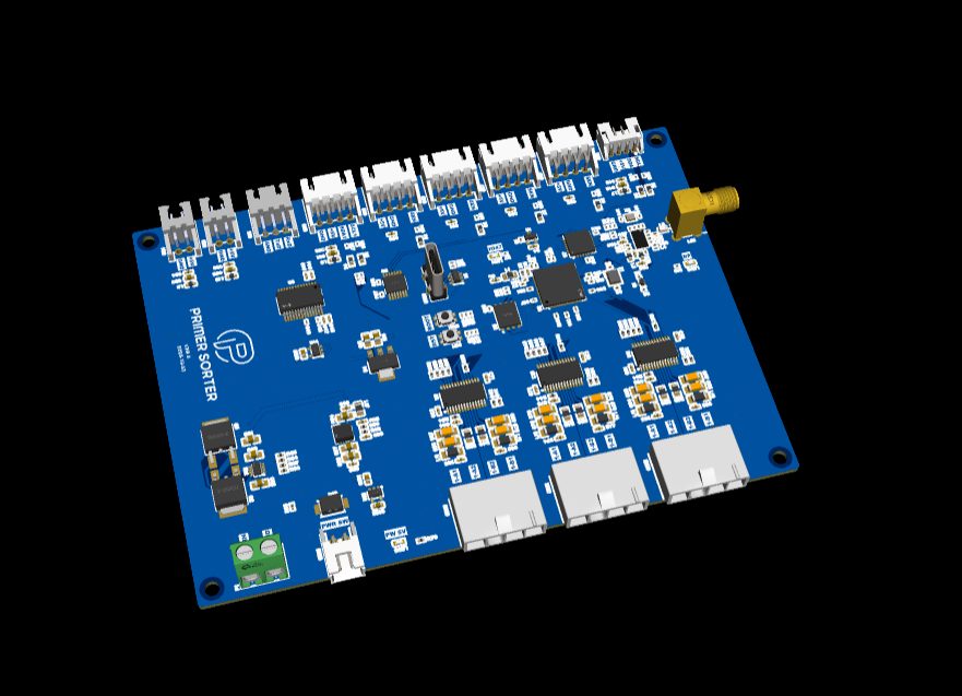
PCB Design
I used EasyEDA Pro for designing schematics and PCB. All components including RP2354B were chosen from JLCPCB’s SMT Part Library.
As I’ve designed and tested several RP2040 and RP2350 boards before, most of the design was trivial and straightforward for me. The only challenging part was for Wi-Fi / Bluetooth chip CYW43439.
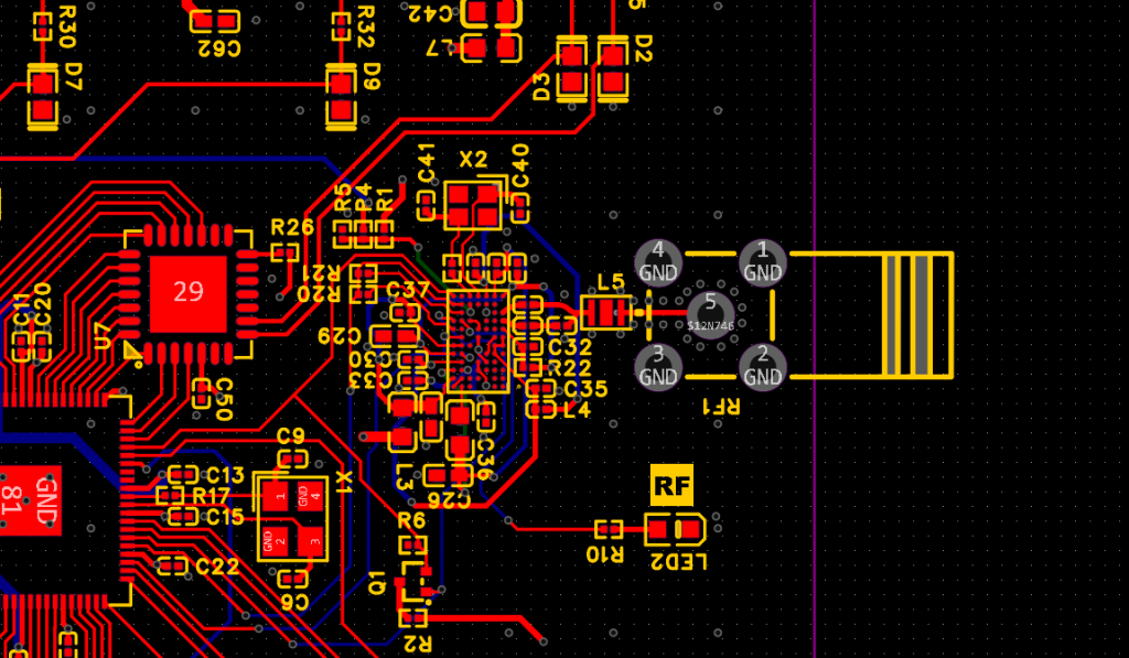
- This chip was in BGA package, WLBGA-63. As I had to design the board for all components being on the top side only, it was not easy to place bypass capacitors in the right way.
- I was referencing the schematics of Raspberry Pi Pico 2W, which was using RP2350A. Because we’re using the RP2350B with a little different GPIO numbering, I should think about what pins to use for the wireless chip. Though I managed to connect it, I would only know the correctness after the PCBA prototyping had completed.
- I could not be confident about using PCB antenna, because the board was a way bigger than the official Raspberry Pi Pico 2W. And the board will have many wires going around IO ports. Thus, I decided to use SMA connector for external antenna usage.
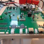
PCBA Prototyping
As I’ve designed the board with all components in JLCPCB SMT Part Library, my client ordered it directly from the JLCPCB’s website. As always, JLCPCB was quick for assembling it. They delivered the fully assembled board in 13 days, including shipping to by client in the United States.
I don’t know / don’t like to judge if JLCPCB’s PCBA quality is better or worse than other competitors. Most of my designs were not much advanced. My designs were mostly in 4-layer stackup, with all through-hole vias, and 0201 or bigger chip components. For this type of PCB design, I believe that any PCBA company can deliver well-working boards. So quicker lead time is more benefit for me and JLCPCB was the fastest, as far as I tried.
Basic testing worked fine. My client was able to flash firmware to the flash memory using RP2350B’s USB port on the PCB. Further testing like Wi-Fi/Bluetooth and stepper motor driving latency needed much firmware development work, yet to be done (at this time of writing).